Here you can learn pcb footprint creation using cadence allegro
Footprint flow
- Padstack creation using pad design.
- pins placement.
- assembly outline
- silkscreen outline
- reference designator
- Draw place bound top area
- Draw DFA bound top area
- Draw no probe top area
Let’s start creating footprint using cadence allegro I am taking sot23 package for reference

Image 1

Image 2
Create one folder in your system name it as pcb library like–>D:\pcb library,Now we are going to create pad in pad designer.
Open pad designer—>
Start—>all programs—>Cadence—>Release 16.3—>PCB Editor Utilities—>Pad designer
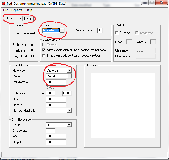
Image 3
Now we opened pad designer
Units : we can change units shown with red circle I want to create it in mm.
Drill/slot hole : we need smd pads for our footprint so put drill diameter as ‘0’(zero)
Next go to layers

Image 4
- Select single layer mode
- Select begin layer
- Give pad dimensions in regular Pad area
Geometry–> Rectangle
Width——->0.7 (Given in land pattern)
Height——>1 (Given in land pattern)
- Now select slodermask_top
Width—–> 0.7 (same as pad width)
Height—–>1 (same as pad height)
- Now select pastemask_Top
Width—–> 0.7 (same as pad width)
Height—–>1 (same as pad height)

Image 5
Now we have created pad just go to file—>save as—-> browse library folder(created beginning of this process) save with name as ‘R0_7X1.pad’.
Now we are going to create this footprint in cadence allegro
Open PCB Editor go to windows—>all programs—>Cadence—>Release 16.3—>PCB Editor
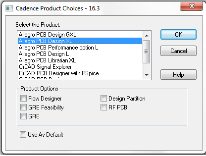
Image 6
Select PCB Design XL then press ok.

Image 7
- we have opened Allegro PCB Design XL Now go to File–>New in that
- Drawing name ‘SOT23’ then click on browse and go to PCB Libraries folder click Open
- In drawing type select ‘Package symbol’
- Click ok
Now set Pad path and psm path go to setup—>user preference—>Paths—>Library—>set path for ‘padpath’ and ‘psmpath’ click on areas shown in red circles then select ‘PCB Libraries’ folder.

Image 8
Set units of your board to MM
- Go to ‘set up—>Design parameter editor’ in that change design units to Millimeter
Now we are going to place pins as shown in SOT23 land pattern
- Go to layout—>pins ‘or’ select Add pin icon on menu bar
- On the right we can see option tab in that give your pad name i.e. r0_7x1
Shown in circles
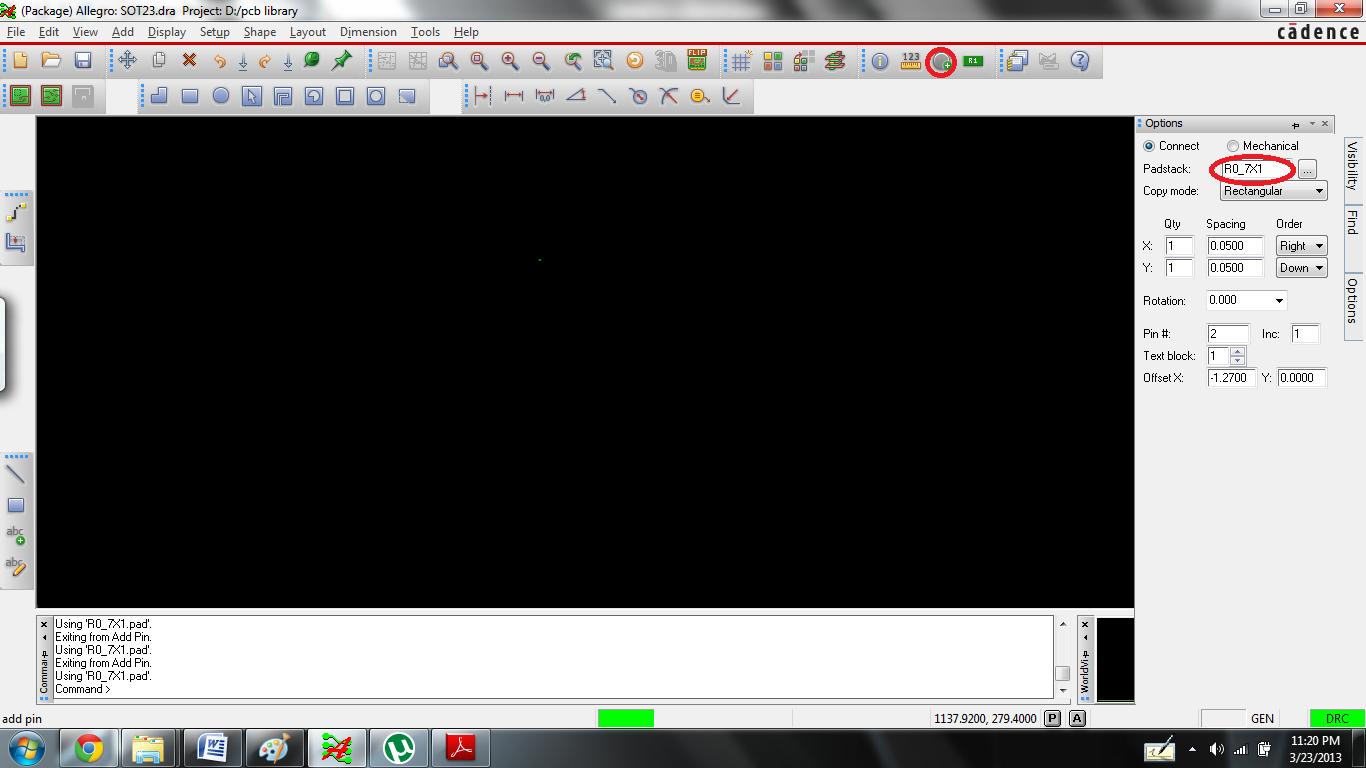
Image 9
Lets place pins
- Type command as x -0.95 -1.2 (you can copy paste this command)
- If you Are unable to see placed pin just press F2 button(zoom fit) on your key board.
- We have placed pin no 1
- Type command x 0.95 -1.2 (you can copy paste this command)
- We have placed pin no 2
- Type command x 0 1.2 (you can copy paste this command)
- Now we have placed total 3 pins as shown in image.
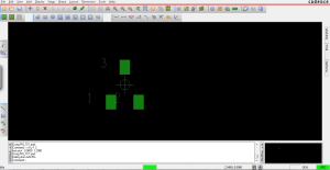
Image 10
Draw Assembly outline
- Take component dimensions from data sheet that is 3.1 x 1.8(maximum values)
- On menu bar ‘Add—>Line’
- On right side go to options select class as package geometry and sub class as assembly top then set line width to 0.2
- Now enter command as “x 1.55 0.9”
- Next enter command as “ix -3.1”—> “iy -1.8” —> “ix 3.1” —>”iy 1.8”

Drawing silkscreen outline is same as assembly but in options select class as package geometry and subclass as silkscreen top.
Place bound outline
- let us take place bound outline same as assembly outline that is 3.1 X 1.8
- on menu bar ‘shape —>filled shape’
- On right side go to options select class as package geometry and sub class as place_bound_top
- Now enter command as “x 1.55 0.9”
- Next enter command as “ix -3.1”—> “iy -1.8” —> “ix 3.1” —>”iy 1.8”

Reference Designator
- On menu bar ‘add—>Text’
- In options select class as ref des and sub class as silkscreen_top
- Click outside of footprint enter text “*”
- Now go to options select sub class as assembly_top
- Click center of footprint enter text ” *”

Now you have created sot23 footprint if you any doubts or suggestions please leave a reply
We are offering online pcb layout training. interested people can contact us at gvsatish11@gmail.com

Nice guide,helped me alot, but i spent some time figuring out the “place command” “x”
for a person who dont know much about PCB production it is a bit hard to figure out all these classes and subclasses, maybe a list of use would be nice.
Thanks for your comment william, sure i will try to make it more brief to help many beginners like you
Hi, is there a way to import stp files in cadence? This will make footprint creation more faster.
I think there no such option
Oh, my god, you are so kind, this is a wonderful guide. Thanks a lots to the writers.
Welcome Hein
how to place pins? when i tried according to your commands. its showing like,”Pick is outside the extent of the drawing … pick again.” please help me…
thank you…
Means you are trying to place it out side the page…for this you have to increase your page extents from menu go to setup–>Design Parameters–>Design(from menu)–>Extents in that change width and Height of page.
thank u..
Plz .. tel me..How to create bried and blind Vias using Allegro pad designer